Material Absorbs Nearly 100% of IR Light
Material Absorbs Nearly 100% of IR Light

CAMBRIDGE, Mass., Nov. 27, 2012 — An ultrathin, tunable device developed at Harvard absorbs 99.75% of infrared light on demand and, when activated, looks like a black blob to IR cameras. The near-perfect absorber could expand the possibilities for energy harvesting and thermal detection.
Designed by scientists at the School of Engineering and Applied Sciences (SEAS) and at the University of California, San Diego, the instrument is composed of a 180-nm-thick layer of vanadium dioxide on a sheet of sapphire.
Although scientists have created many perfect absorbers before, none have had such versatile properties, the team said. When two mirrors sandwich an absorbing material in a Fabry-Perot cavity, for instance, light simply reflects back and forth until it is mostly gone. Other devices employ surfaces with nanoscale metallic patterns that trap and eventually absorb the light.
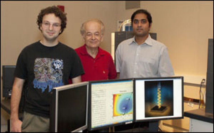
From left, Mikhail Kats, Federico Capasso and Shriram Ramanathan used unusual materials and interference effects to create a perfect absorber. They are pictured here in a scanning electron microscopy imaging suite at the Harvard Center for Nanoscale Systems. Courtesy of Caroline Perry, SEAS Communications.
“Our structure uses a highly unusual approach, with better results,” said principal investigator Federico Capasso, Robert L. Wallace Professor of Applied Physics and Vinton Hayes Senior Research Fellow in electrical engineering at SEAS. “We exploit a kind of naturally disordered metamaterial, along with thin-film interference effects, to achieve one of the highest absorption rates we’ve ever seen. Yet our perfect absorber is structurally simpler than anything tried before, which is important for many device applications.”
Capasso’s team worked with scientists at Harvard and UCSD to take advantage of the surprising properties of the two materials they used.
Vanadium dioxide is typically an insulating material; i.e., it does not conduct electricity well. But it does undergo a dramatic transition when taken from room temperature to about 68 °C. As the temperature approaches a critical value, the crystal rearranges itself, and metallic islands appear as specks, scattered within the material. More metallic islands appear until the material becomes uniformly metallic.
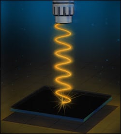
Artist's rendition of the experimental setup used to measure the reflectivity of the vanadium-sapphire device. Modified from an illustration by Kirill Nadtochiy.
“Right near this insulator-to-metal transition, you have a very interesting mixed medium, made up of both insulating and metallic phases,” said SEAS associate professor of materials science Shriram Ramanathan, who synthesized the thin film. “It’s a very complex and rich microstructure in terms of its electronic properties, and it has very unusual optical properties.”
When manipulated correctly, those properties are ideal for infrared absorption.
The underlying sapphire substrate, meanwhile, has a major role as well. While usually transparent, its crystal structure actually makes it reflective and opaque, like a metal, to a narrow subset of infrared wavelengths. As a result, the combination of materials internally reflects and “devours” incident infrared light.
“Both of these materials have lots of optical losses, and we’ve demonstrated that, when light reflects between glossy materials, instead of transparent or highly reflective ones, you get strange interface reflections,” said SEAS graduate student Mikhail Kats. “When you combine all of those resulting waves, you can coax them to destructively interfere and completely cancel out. The net effect is that a film one hundred times thinner than the wavelength of the incident light can create perfect absorption.”

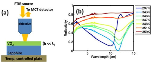
Left: The experimental setup used for measuring the reflectivity of the vanadium-sapphire device. The vanadium oxide layer is only 180 nm thick, much thinner than the wavelength of the incident infrared light. Right: At just the right temperature (light blue line), the reflectivity of the device drops almost to zero (99.75% absorbance) for infrared light at a wavelength of 11.6 µm. Courtesy of Mikhail Kats.
The great challenge was not only to understand this behavior, but also to discover how to fabricate pure enough samples of the vanadium dioxide.
Ramanathan said vanadium oxide can exist in many oxidation states but only goes through a metal-insulator transition with vanadium dioxide close to room temperature. To grow the complex films, the researchers developed several techniques to allow “exquisite compositional and structural control, almost at the atomic scale.” The resulting phase enabled the researchers to observe the remarkable properties, which otherwise would have been difficult to see.
Because the device can be switched easily between its absorbent and nonabsorbent states, it is suitable for a variety of applications, including thermal imaging devices (bolometers) with tunable absorption, spectroscopy devices, tunable filters, thermal emitters, radiation detectors and energy-harvesting equipment.
“An ideal bolometer design needs to absorb all of the infrared light that falls on it, turning it to heat, and, correspondingly, its resistance should change a lot per degree change in temperature,” Kats said. “In principle, our new perfect absorber could be used to make incredibly sensitive thermal cameras.”
Details of the device were published in Applied Physics Letters.
For more information, visit: www.seas.harvard.edu


